Introduction
The block diagram shown below represents a voting booth monitoring system. For privacy reasons, a voting booth can only be used if the booth on either side is unoccupied. The monitoring system has four inputs and two outputs. Whenever a voting booth is occupied, the corresponding input (A, B, C, & D) is a (1). The first output, Booth, is a (1) whenever a voting booth is available. The second output, Alarm, is a (1) whenever the privacy rule is violated.
Introduction
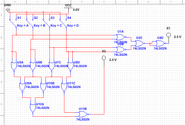
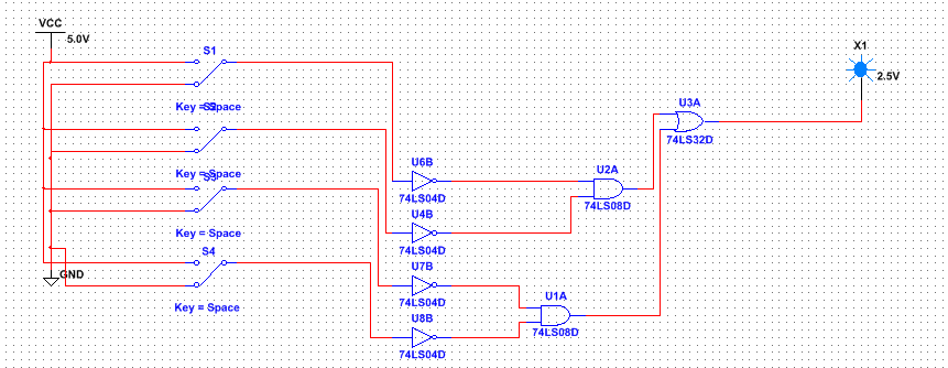
In this activity you will revisit the voting booth monitoring system introduced in Activity 2.2.2 NAND Logic Design. Specifically, you will be implementing the NOR only combinational logic circuits for the two outputs Booth and Alarm. In terms of efficiency and gate/IC utilization, these NOR only designs will be compared with the previously designed AOI and NAND implementations.
The block diagram shown below represents a voting booth monitoring system. For privacy reasons, a voting booth can only be used if the booth on either side is unoccupied. The monitoring system has four inputs and two outputs. Whenever a voting booth is occupied, the corresponding input (A, B, C, & D) is a (1). The first output, Booth, is a (1) whenever a voting booth is available. The second output, Alarm, is a (1) whenever the privacy rule is violated.
Introduction
In this activity you will revisit the voting booth monitoring system introduced in Activity 2.2.2 NAND Logic Design. Specifically, you will be implementing the NOR only combinational logic circuits for the two outputs Booth and Alarm. In terms of efficiency and gate/IC utilization, these NOR only designs will be compared with the previously designed AOI and NAND implementations.
in the process of converting NAND/NOR through AOI was just a process of trial and error from taking items out and testing to counting IC chips to see how they work comparing both of the schematics i saw that they both used less Items than normal which i found intresting.
How did we do it?
We converted the AOI logic to a circuit using universal gate design the NAND and NOR gates. We had to find the AND OR and INVERTER to the NAND and NOR gates. We then changed the AOI gates with either NAND and NOR gates.
We converted the AOI logic to a circuit using universal gate design the NAND and NOR gates. We had to find the AND OR and INVERTER to the NAND and NOR gates. We then changed the AOI gates with either NAND and NOR gates.
